A finding that enables graphene to better absorb light could be the key manufacturers have been waiting for to utilize the super-strong, superlight material in next-generation devices including light detectors, touchscreens, glucose testing meters and even water filtration systems.
For the first time, the UCF team demonstrated more than 45 percent absorption of light in a single layer of graphene –single atom thick material. This may make it possible to use the material for applications that require the incident light to be fully utilized.
Debashis Chanda, a researcher in the NanoScience Technology Center and College of Optics and Photonics and Michael N. Leuenberger, a researcher in the NanoScience Technology Center, Department of Physics, and College of Optics and Photonics, and their teams published their findings in the Physical Review B journal .
“This is the first published work on extremely high light absorption in graphene which is tunable dynamically,” Chanda said.
“Theoretical studies show further design optimization can lead to further enhanced absorption close to 90 percent,” Leuenberger said.
The UCF teams received $544,000 from the Defense Advanced Research Agency’s (DARPA) Wafer Scale Infrared Detectors program (WIRED) Phase-I for 18 months. Recently the teams also obtained a Phase-II award for $419,000 to continue its work over the coming 12 months.
Research with graphene has increased since the physicists who researched its properties were awarded with a Nobel Prize in 2010.
Graphene alone has very poor light absorption – less than two percent, and researchers have focused on ways to increase that percentage to make the material functional. Previous efforts have used metal particles on graphene sheets to show enhanced light absorption, but in those cases the majority of the light was absorbed by the metal, thus defeating the purpose. Chanda said he and his team members did not attempt to alter the properties of the graphene in any way. Instead, they placed the graphene on a polymer substrate as a support layer and stamped it using a polymeric stamp to form a nanoscale pattern on the pristine graphene. An optical cavity stopped light from escaping and repeatedly bounced light back to the patterned graphene layer and enhanced light absorption.
In addition, the process allows voltage driven change in electron energy and thus in the electron density, enabling absorption of different wavelengths of light – making the process dynamically tunable.
Chanda and Leuenberger said the work is of special interest to DARPA because of the need for tunable infrared cameras that can operate at room temperature and can be used to develop multispectral night vision equipment, gas and chemical sensors. A multispectral imaging capability will enable infrared imaging across various bands with the same camera, revealing further detailed information about the object – important for space exploration and many United Stated Department of Defense specific applications.
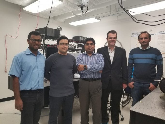
Other team members are post-doctoral fellow Sayan Chandra, the lead doctoral student Alireza Safaei and the doctoral students Mahtab Khan and Muhammad Waqas Shabbir, all researchers in the NanoScience Technology Center.
