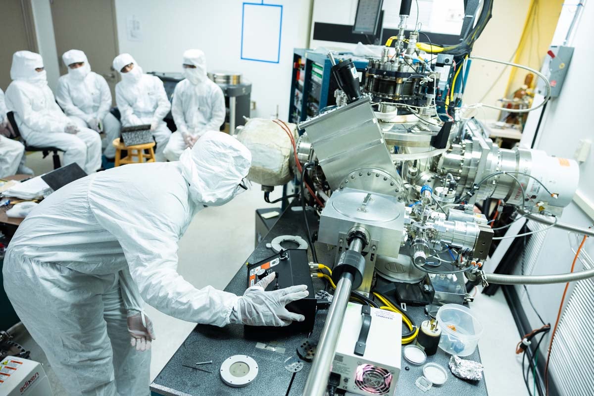
At the heart of every electronic device is a semiconductor chip. These tiny circuits can improve fuel efficiency in your car, allow your computer to process and store data, or enable you to download the latest apps on your phone. But the process of manufacturing semiconductor chips is tricky and ripe for improvement. One small mistake can cost millions, but advanced technology can help eliminate flaws during fabrication and transform the industry overall.
UCF will aid in the development of this technology through a new regional research hub led by the University of Florida. The goal is to use digital twins, virtual representations of physical objects or processes, to optimize semiconductor manufacturing. The Florida/Caribbean hub is one of seven research hubs across the U.S. that comprise the Manufacturing USA institute called SMART USA, which was funded through a $285 million award from the federal administration earlier this year.
The funding was highly competitive and is a result of the U.S. Department of Commerce’s CHIPS Manufacturing USA Institute competition, which selected the SMART USA proposal from dozens of entries. SMART, which stands for Semiconductor Manufacturing and Advanced Research with Twins, is led by the Semiconductor Research Corporation.
“The focus of this hub is going to be on digital twins,” says Professor Reza Abdolvand, the chair of the Department of Electrical and Computer Engineering who co-led UCF’s portion of the proposal alongside Grace Bochenek ’98PhD, the executive director of the Pegasus Research Institute and the director of the Institute for Simulation and Training. “The goal is to accurately virtualize the manufacturing process so we can find out what could go wrong before starting the costly and time-consuming manufacturing process.”
The Problems With Semiconductor Manufacturing
Semiconductor chips aren’t simple to make. They are fabricated in huge facilities called semiconductor fabrication plants which consist of highly controlled environments called cleanrooms. Here, the air is constantly filtered to remove small particles that could create defects in the final product. Most chips are made from silicon wafers, which are more brittle than glass, and the process of turning these silicon substrates into semiconductor chips is lengthy and complex — it can take hundreds of steps and up to six months to produce one batch of silicon wafers from start to finish.
“Mistakes in this process are very expensive and they can be made in many steps,” Abdolvand says. “In the design, for example — if what you design is faulty, the end product will be faulty and you could lose billions of dollars.”
Currently, the industry can and does use modeling and simulation in the design process, so they can better predict if the final product will work as intended. But this technology has not caught up to the manufacturing process.
“Manufacturing is basically trial and error until you’re happy with what you see,” Abdolvand says. “The hope is to extend the modeling concept to what the tool can do with the substrate. What if we can simulate what the tool does before it happens?”
The tools used in the manufacturing process can become outdated and obsolete very quickly, which have also posed challenges for the industry, specifically increasing the modeling reiteration cost for manufacturing.
UCF’s Role in the Research Hub
Advances in artificial intelligence and machine learning now allows for development of realistic models that could solve the semiconductor industry’s challenges. AI-enabled digital twins can be used to mimic the manufacturing process, allowing tech businesses to predict what errors could be made before they occur, saving both time and money.
Abdolvand and Bochenek are leading the charge for the university. Together, ECE and IST researchers will gather, collect, analyze and interpret data that can be used to create a digital twin.
“We’re excited about this partnership and UCF’s contributions to SMART USA’s effort to achieve national security goals through innovative digital transformation,” Bochenek says. “This region will be key in ensuring the U.S. global competitive advantage in this semiconductor chip manufacturing.”
Bringing semiconductor manufacturing to the U.S. is a key goal for the institute, to not only remain dominant in the global market, but to be more cost effective.
“The largest companies with semiconductor business are in the U.S. They do the design here, but the manufacturing is outside the U.S.,” Abdolvand says. “The plan is to bring manufacturing back to the U.S. If manufacturing cost could be reduced through digital twining, manufacturing can be done in the U.S. and still be very cost competitive.”